About this Data Sheet
Purpose and Scope
The GM02SP is a complete LTE Cat M1/NB1/NB2 module including baseband, RF, low-power GNSS and memory, for the design of narrowband low data rate M2M and IoT devices for wide deployment. This document provides technical information about GM02SP LGA module. GM02SP is based on Sequans’s Monarch 2 platform.
Who Should Read this Document?
This document is intended for engineers who develop User Equipment (UE) for LTE systems, with embedded location processing using GNSS technology.
Changes in this Document
This revision 13 of the document supersedes revision 12.
| Revision | Date | Changes from the previous version |
|---|---|---|
| 13 | Jan. 2026 |
|
| 12 | 2025 |
|
| 11 | Oct. 2024 |
|
| 10 | July 2024 |
|
| 9 | June 2024 |
|
| 8 | Jan. 2024 |
|
| 7 | Oct. 2023 |
|
| 6c | Jan. 2023 | Add new P/N and corrections to table 2. Adjust the weight in section 4 |
| 6b | Oct. 2022 | Erratum to section 1.4 |
| 6a | Sept. 2022 | Erratum on software version in table 2 |
| 6 | Aug. 2022 | Mechanical characteristics changes to account for new hardware (thickness) in chapter 4 |
| 5 | July 2022 |
|
| 4 | April 2022 |
|
| 3 | March 2022 |
|
| 2 | Jan. 2022 |
General Description
The Monarch 2 GM02SP is an LTE Cat M1/NB1/NB2 module based on Sequans' second generation Monarch 2 chip platform. GM02SP is a total module solution, including a complete, Single-SKU™ RF front end for deployment in any band worldwide, and an integrated EAL5+ Secure Element (SE) enabling the integration of the SIM inside the module with zero compromise on security while lowering cost and reducing complexity. The GM02SP is part of Sequans next generation "S" family of modules, featuring a very small yet cost-effective form factor that requires no external components. The “P” variant in the part number stands for the additional Low-Power GNSS functionality. The GM02SP maintains pin-to-pin compatibility w/r to the legacy GM02S.
The GM02SP leverages Sequans’s 15-plus years of experience in 4G+ technologies and incorporates Sequans’s carrier-approved LTE protocol stack and a software suite amongst the most mature in the industry. The GM02SP is part of Sequans’s next generation "S" family of modules, featuring a very small and cost-effective form factor which requires no external components. The GM02SP inherits Monarch’s already certified LTE-M and NB-IoT stack and delivers a significantly improved performance and lower power consumption thanks to Sequans’s second generation Monarch 2 chip and the new module architecture.
Sequans’s technology, both hardware and software, is completely owned by Sequans, ensuring a fast time to market and the lowest total cost of ownership for device makers.
Frequency Bands
| Band | Name | Limits (MHz) |
|---|---|---|
| B1 | IMT | 1920 – 1980 |
| B2 | PCS | 1850 – 1910 |
| B3 | DCS | 1710 – 1785 |
| B4 | AWS-1 | 1710 – 1755 |
| B5 | Cellular | 824 – 849 |
| B8 | Extended GSM 900 | 880 – 9151 |
| B12 | Lower SMH | 699 – 716 |
| B13 | Upper SMH | 777 – 787 |
| B17 | Lower SMH | 704 – 716 |
| B18 | Lower 800 | 815 – 830 |
| B19 | Upper 800 | 830 – 845 |
| B20 | 800 Digital Dividend | 832 – 862 |
| B25 | Extended PCS | 1850 – 1915 |
| B26 | Extended Cellular | 814 – 849 |
| B28 | APT | 703 – 748 |
| B66 | Extended AWS | 1710 – 1780 |
| B85 | Extended Lower SMH | 698 – 716 |
The GM02SP monitors the L1 band (at 1,575.42 MHz) for GNSS applications.
Applications
The GM02SP is ideal for adding LTE-M and/or NB-IoT LTE connectivity to narrow band, low data rate M2M and IoT devices such as utility meters, industrial sensors, health and fitness appliances, asset trackers, and many additional devices in smart home, smart city, and wearable applications.
The GM02SP can also be used as a slim modem controlled by an external MCU via its UART. Alternatively, the GM02SP can execute applets on its embedded MCU.
The LP-GNSS functionality uses on-chip or cloud-assisted mode to locate the IoT device.
The GNSS processing tracks the GPS and Galileo constellations and can be activated when the LTE modem is
not in function (AT+CFUN=0).
Block Diagram
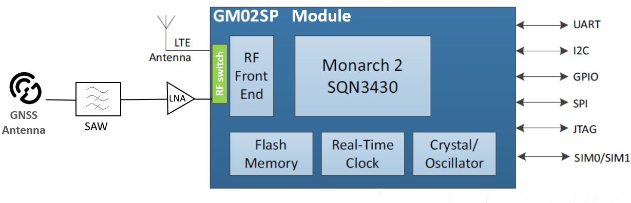
General Features
| Physical Characteristics | LGA module, 120 pads.
Size: 16.3 × 17 × 2.3 mm |
| Temperature Range |
Operation temperature range: -40 to +85 °C Storage: MSL3 |
| Power Supply |
Voltage range for RF compliance: 2.5 to 5.5 V Functional voltage range: 2.2 to 5.5 V |
| Tx Power | +23 dBm in each band |
| Interfaces |
|
| SMS | Text and PDU modes |
| Firmware Upgrade | UART interface, FOTA, support of full and differential firmware upgrade |
| RoHS/REACH | All hardware components fully comply with EU RoHS and REACH directives, bromine-free |
| GNSS Features | Low-power location processing, performed either fully on-chip, or with cloud
assistance*.
*Cloud assistance = satellites’ ephemerides and almanacs downloaded from cloud into the device. Important:
The GNSS functionality is available only if the LTE modem is off
( AT+CFUN = 0). |
| LTE Features |
|
Available Part Numbers
GM02SP’s ECCN is 5A991.
| Part Number | Hardware Version | Software Build (ATI1) | UE Version (ATI1) | PTCRB Model Name / Model | SVN | Availability Status |
|---|---|---|---|---|---|---|
| GP02RBAQRC | HW Rev. 3 | LR 8.0.6.3 | UE 8.0.6.3 | GM02SP | 13 | Obsolete, engineering release, not available any more |
| GP02RBAQRD | ||||||
| GP02RBAQRE | LR 8.2.0.0 | UE 8.2.0.0 | 13 | |||
| GP02RBAQRF | LR 8.2.0.3 | UE 8.2.0.3 | 15 | Available, OTP unlocked | ||
| GP02RBAQRG | LR 8.2.1.0 | UE 8.2.1.0 | 19 |
Interfaces
The GM02SP provides electric interfaces connecting it to the external parts, such as communication I/O ports, GPIO and antenna RF I/O. This chapter provides information about all these interfaces.
Power supply pins and details thereof are detailed in section Electrical, RF and Thermal Characteristics.
- Default assigned function;
- State during low power modes;
- Configuration with AT commands;
- Pull status and requirements.
Pin Assignment
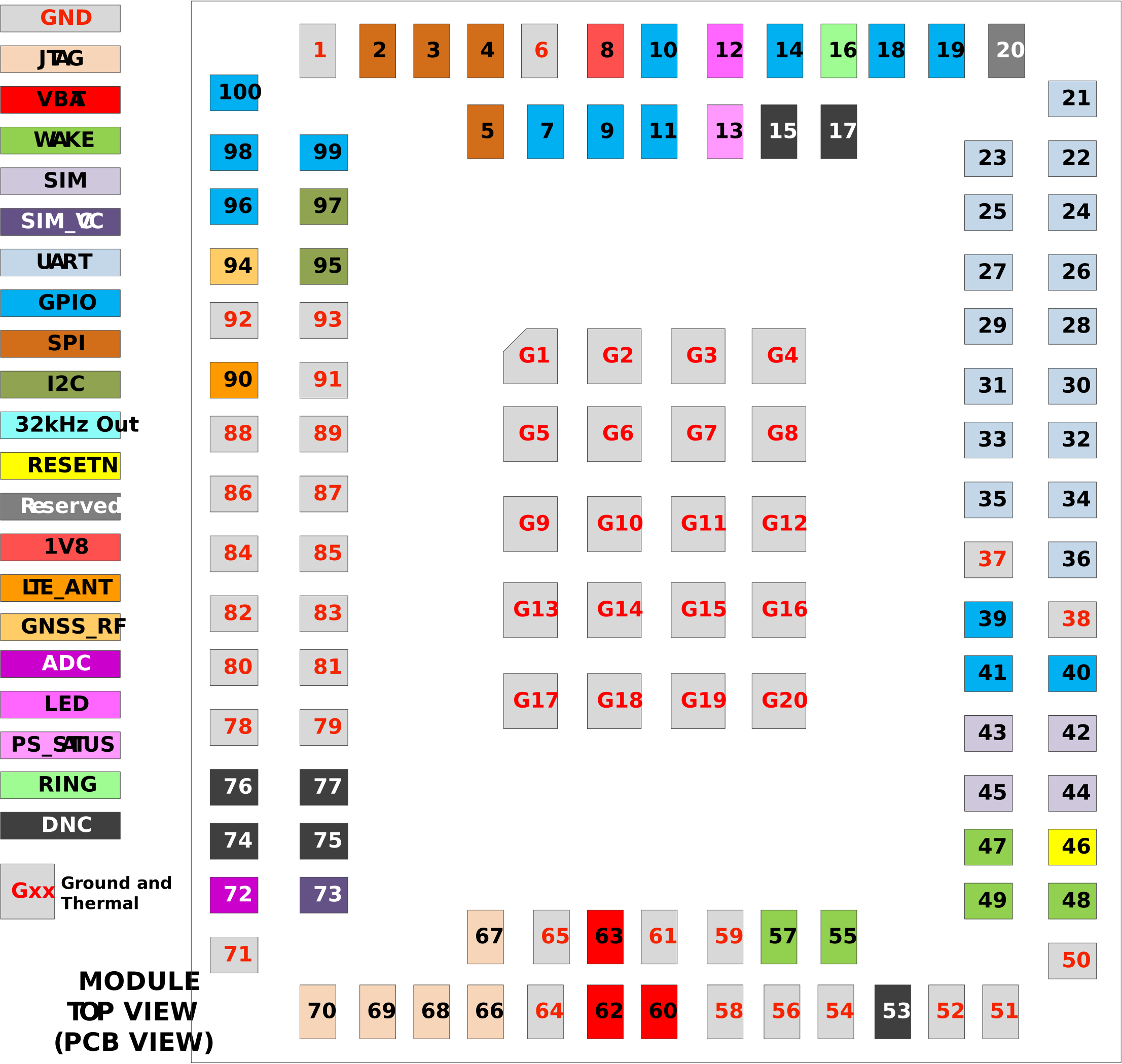
UART
The GM02SP has three available UARTs to communicate with the application processor.
| Pad # | Pad Name | Primary Function | Alternate2 Function | Power Group | Dir. | Pad type3 | Reset state |
|---|---|---|---|---|---|---|---|
| 36 | GPIO12/TXD0 | TXD0 | GPIO12 | PVDD_1V8 | In/Out | BIDIR | High-Z |
| In for primary function, UART0 | |||||||
| 34 | GPIO13/RXD0 | RXD0 | GPIO13 | PVDD_1V8 | In/Out | BIDIR | Out |
| Out for primary function, UART0 | |||||||
| 35 | GPIO14/CTS0 | CTS0 | GPIO14 | PVDD_1V8 | In/Out | BIDIR | Out |
| Out for primary function, UART0 | |||||||
| 33 | RTS0 | RTS0 | N/A | PMU_5V | In | IN | High-Z |
| Wake signal enabled by default. | |||||||
| 32 | TXD1 | TXD1 | N/A | PVDD_1V8 | In | BIDIR | High-Z |
| UART1 | |||||||
| 30 | RXD1 | RXD1 | N/A | PVDD_1V8 | Out | BIDIR | Out |
| UART1 | |||||||
| 31 | CTS1 | CTS1 | N/A | PVDD_1V8 | Out | BIDIR | Out |
| UART1 | |||||||
| 29 | RTS1 | RTS1 | N/A | PMU_5V | In | IN | High-Z |
| Wake signal enabled by default. | |||||||
| 28 | GPIO15/TXD2 | TXD2 | GPIO15 | PVDD_1V8 | In/Out | BIDIR | High-Z |
| In for primary function, UART2 | |||||||
| 26 | GPIO16/RXD2 | RXD2 | GPIO16 | PVDD_1V8 | In/Out | BIDIR | Out |
| Out for primary function, UART2 | |||||||
| 27 | GPIO17/CTS2/DCD0 | GPIO17 | CTS2/ DCD0 | PVDD_1V8 | In/Out | BIDIR | Out |
| UART2 | |||||||
| 25 | GPIO18/RTS2/DSR0 | GPIO18 | RTS2/ DSR0 | PVDD_1V8 | In/Out | BIDIR | High-Z |
| UART2 | |||||||
| 24 | GPIO19/TXD3 | GPIO19 | TXD3 | PVDD_1V8 | In/Out | BIDIR | HighZ |
| In for primary function, UART3 | |||||||
| 22 | GPIO20/RXD3 | GPIO20 | RXD3 | PVDD_1V8 | In/Out | BIDIR | Out |
| Out for primary function, UART3 | |||||||
| 21 | GPIO21/CTS3 | GPIO21 | CTS3 | PVDD_1V8 | In/Out | BIDIR | Out |
| UART3 | |||||||
| 23 | GPIO22/RTS3 | GPIO22 | RTS3 | PVDD_1V8 | In/Out | BIDIR | Out |
| UART3 | |||||||
UART Default Configuration
- The Host-Modem interface, also named ‘AT mode’, configures and exchanges data with the modem using standard or proprietary AT commands. This mode requires a high-speed UART port with flow control.
- The Modem Console interface copies the logs from the LTE modem.
- The Debug interface (also referred to as DCP) is needed by the DM Tool during design verification or debugging. This interface can be used to upgrade the software using SFU.
The default configuration appears in Table 5.
| UART# | Baudrate | Flow Control | Application | Wake Source | Manufacturing Upgrade |
|---|---|---|---|---|---|
| 0 | 115200 | Enabled | AT | Yes | Yes |
| 1 | 921600 | Enabled | AT | Yes | Yes |
| 2 | 115200 | Disabled | Console | No | No |
Refer to the Module Manufacturing Guidelines for overriding this default configuration.
UART wiring
The GM02SP complies to the DCE-DTE convention for UART lines. It is designed as a DCE (Data Communication Equipment).
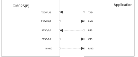
The output from the device at one end of the link connects to the corresponding input at the other end of the link and vice versa. The Figure 3 represents the typical implementation for the UART connection (including hardware flow control in case of high-speed UARTs).
- Port TxD on the application board side sends data to the GM02SP's TxD signal line.
- Port RxD on the application board side receives data from the GM02SP's RxD signal line.
-
CTS0, CTS1, CTS2, CTS3: Clear-To-Send signals of resp.
UART0, UART1, UART2, UART3 (active low). To be connected to the CTS of the remote UART
device. See Figure 3.
Leave CTS unconnected if hardware flow control is not used.
- RTS0, RTS1, RTS2, RTS3: Ready-To-Send signals of resp. UART0, UART1, UART2, UART3 (active low). To be connected to the RTS of the remote UART device. Tie to a 1 kΩ pull-down when flow control is not used. If connected to an external part (like a RS 232 driver), the user must insure that the part presents a low level to the GM02SP See Figure 3.
Figure 3 represents the typical implementation for hardware flow control.
Various UART-to-USB converters were tested on GM02S/GM02SP modules, including the Exar XR21V1410, FTDI FT234XD or FTDI FT4232H. Implementation examples can be found in reference designs schematics.
USIM Interfaces
SIM0 Interface
| Pad # | Pad Name | Primary Function | Power Group | Dir. | Pad type 4 | Reset State |
|---|---|---|---|---|---|---|
| 42 | SIM0_CLK | SIM0_CLK | PVDD_1V8 | Out | BIDIR | Out |
| 45 | SIM0_DETECT5 | SIM0_DETECT | PMU_5V | In | IN | High-Z |
| 44 | SIM0_IO | SIM0_IO | PVDD_1V8 | In/Out | BIDIR | High-Z |
| 43 | SIM0_RSTN | SIM0_RSTN | PVDD_1V8 | Out | BIDIR | Out |
| 73 | SIM0_VCC6 | SIM0_VCC | PVDD_1V8 | Out | SUPPLY | Out7 |
SIM1 Interface
| Pad # | Pad Name | Primary Function | Alternate Function | Power Group | Dir. | Pad Type 8 | Reset state |
|---|---|---|---|---|---|---|---|
| 40 | GPIO26/SIM1_CLK | GPIO26 | SIM1_CLK | PVDD_1V8 | Out | BIDIR | Out |
| 41 | GPIO27/SIM1_RESETN | GPIO27 | SIM1_RESETN | PVDD_1V8 | Out | BIDIR | Out |
| 39 | GPIO25/SIM1_IO | GPIO25 | SIM1_IO | PVDD_1V8 | In/Out | BIDIR | High-Z |
Miscellaneous Hardware Considerations
- Use a 100 nF decoupling capacitor on SIM_VCC.
- Use a 4.7 kΩ pull-up resistor between SIM_VCC and SIM_IO.
- The SIM connector should be located as close as possible to the module.
- Please ensure ground continuity between the SIM card and the module.
- If the application handles SIM card hot swapping, the SIM slot must contain a card detector in order for the software to process the event immediately. Default software configuration is to support SIM_DETECT.
- If the SIM card tray does not support SIM_DETECT (not recommended), keep the SIM_DETECT signal high and configure the module for SIM card detection using polling mode.
I²C
| Pad # | Pad Name | Primary Function | Alternate Function | Power Group | Dir. | Pad type 9 | Reset State |
|---|---|---|---|---|---|---|---|
| 95 | GPIO23/I2C_SDA | GPIO23 | I2C_SDA | PVDD_1V8 | In/Out | BIDIR | High-Z |
| 97 | GPIO24/I2C_SCL | GPIO24 | I2C_SCL | PVDD_1V8 | In/Out | BIDIR | High-Z |
PCM
| Pad # | Pad Name | Primary Function | Alternate10 Function | Power Group | Dir. | Pad type 11 | Reset State |
|---|---|---|---|---|---|---|---|
| 96 | GPIO4/PCM_CLK | GPIO4 | PCM_CLK | PVDD_1V8 | In/Out | BIDIR | High-Z |
| 98 | GPIO3/PCM_RXD | GPIO3 | PCM_RXD | PVDD_1V8 | In/Out | BIDIR | High-Z |
| 99 | GPIO5/PCM_FS | GPIO5 | PCM_FS | PVDD_1V8 | In/Out | BIDIR | High-Z |
| 100 | GPIO6/PCM_TXD | GPIO6 | PCM_TXD | PVDD_1V8 | In/Out | BIDIR | High-Z |
SPI
| Pad # | Pad Name | Primary Function | Alternate12 Function | Power Group | Dir. | Pad type 13 | Reset state |
|---|---|---|---|---|---|---|---|
| 3 | GPIO7/SPI_SDI | GPIO7 | SPI_SDI | PVDD_1V8 | In/Out | BIDIR | High-Z |
| 4 | GPIO8/SPI_SDO | GPIO8 | SPI_SDO | PVDD_1V8 | In/Out | BIDIR | High-Z |
| 2 | GPIO9/SPI_CLK | GPIO9 | SPI_CLK | PVDD_1V8 | In/Out | BIDIR | High-Z |
| 5 | GPIO10/SPI_CSN1 | GPIO10 | SPI_CSN1 | PVDD_1V8 | In/Out | BIDIR | High-Z |
| 7 | GPIO11/SPI_CSN214 | GPIO11 | SPI_CSN2 | PVDD_1V8 | In/Out | BIDIR | High-Z |
When SPI is enabled, SPI_SDO (Serial Data Output) is an INPUT which is connected to the slave DO (Data Output). Conversely, SPI_SDI (Serial Data Input) is an OUTPUT connected to the slave's DI (Data Input).
GPIO
| GPIO Range | Default State |
|---|---|
| GPIO3 to GPIO11 | Disabled |
| GPIO17 to GPIO28 | Disabled |
| GPIO31 to GPIO35 | Disabled |
The GPIOs are documented in this data sheet according to their shared or assigned function. In addition to the GPIO, five wake signals are also available (see section Other Signals).
GM02SP GPIO to SQN 3430 GPIO Number Crosstable
AT commands such as AT+SMGI or AT+SMGT which test GPIOs behaviour do
not take the GM02S's GPIO number as parameter, but an internal numbering given below. For example, to
test GPIO1, the GPIO parameter given to AT+SMGI is 38.
| GM02SP GPIO Number | AT Command Corresponding Value |
|---|---|
| 1 | 38 |
| 2 | 39 |
| 3 | 34 |
| 4 | 33 |
| 5 | 32 |
| 6 | 31 |
| 7 | 21 |
| 8 | 22 |
| 9 | 20 |
| 10 | 23 |
| 11 | 24 |
| 12 | 4 |
| 13 | 5 |
| 14 | 6 |
| 15 | 10 |
| 16 | 11 |
| 17 | 13 |
| 18 | 12 |
| 19 | 14 |
| 20 | 15 |
| 21 | 16 |
| 22 | 17 |
| 23 | 18 |
| 24 | 19 |
| 25 | 28 |
| 26 | 29 |
| 27 | 30 |
| 31 | 3 |
| 32 | 1 |
| 33 | 35 |
| 34 | 36 |
| 35 | 37 |
Other Signals
| Pads Type | Pads Number |
|---|---|
| GND | 1, 6, 37, 38, 50, 51, 52, 54, 56, 58, 59, 61, 64, 65, 71,78, 79, 80, 81, 82, 83, 84, 85, 86, 87, 88, 89, 91, 92, 93 |
| DNC (Reserved) | 15, 17, 53, 74, 75, 76, 77 |
| Pad # | Name | Primary Function | Alternate15 Function | Power Group | Dir. | Pad Type16 | Reset State |
|---|---|---|---|---|---|---|---|
| 72 | ADC1 | ADC1 (see below) | N/A | N/A | In | IN | N/A |
| Analogue-Digital Converter (ADC, IN) | |||||||
| 12 | GPIO1/STATUS_LED | STATUS_LED | GPIO1 | PVDD_1V8 | In/Out | BIDIR | High-Z |
| Primary Function: Status LED (STATUS_LED, OUT) | |||||||
| 13 | GPIO2/PS_STATUS | PS_STATUS | GPIO2 | PVDD_1V8 | In/Out | BIDIR | High-Z |
| Primary Function: Power Saving status (PS_STATUS, OUT) enabled by default. Active high. | |||||||
| 14 | LNA_ENABLE | LNA_ENABLE | PVDD_1V8 | In/Out | BIDIR | High-Z | |
| Primary Function: External GNSS LNA enable signal | |||||||
| 19 | GPIO31/PWM0/ 19M2_OUT | GPIO31 | PWM0/19M2_OUT | PVDD_1V8 | In/Out | BIDIR | High-Z |
| 18 | GPIO32/PWM1 | GPIO32 | PWM1 | PVDD_1V8 | In/Out | BIDIR | High-Z |
| 9 | GPIO33/TX_IND | TX_IND | GPIO33 | PVDD_1V8 | In/Out | BIDIR | High-Z |
| Primary Function: Transmission indicator (TX_IND, OUT). Active high. | |||||||
| 10 | GPIO34/ANT_TUNE0 | ANT_TUNE0 | GPIO34 | PVDD_1V8 | In/Out | BIDIR | High-Z |
| Primary Function: Antenna tuning (ANT_TUNE0, OUT) | |||||||
| 11 | GPIO35/ANT_TUNE1 | ANT_TUNE1 | GPIO35 | PVDD_1V8 | In/Out | BIDIR | High-Z |
| Primary Function: Antenna tuning (ANT_TUNE1, OUT) | |||||||
| 20 | RESERVED/FFF_FFH | RESERVED | N/A | PVDD_1V8 | N/A | BIDIR | High-Z |
| Boot mode selection (FFF_FFH, IN). This pad needs a pull-down resistor by default. | |||||||
| 15, 17, 53, 74, 75, 76, 77 | RESERVED | RESERVED | N/A | PVDD_1V8 | N/A | BIDIR | N/A |
| Do not connect | |||||||
| 46 | RESETN | RESETN | N/A | PMU_5V | In | IN | In, Pull-up |
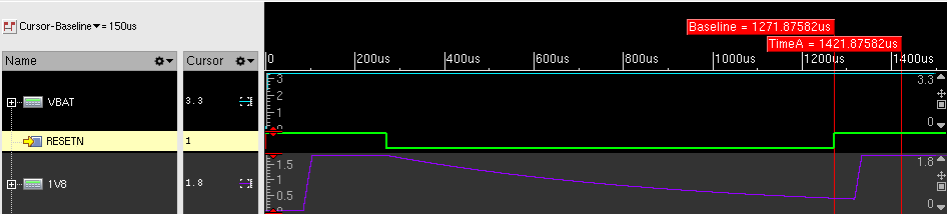
| Module HW reset signal. Active low. The minimum duration of a reset pulse on the RESETN signal is 100 µs. | |||||||
| 16 | RING0 | RING0 | N/A | PVDD_1V8 | In/Out | BIDIR | High-Z |
| UART0 ring line (RING0, OUT). Enabled by default with inverted polarity. | |||||||
| 48 | WAKE0 | WAKE0 | N/A | PMU_5V | In | IN | High-Z |
| Wake #0 input line (WAKE0, IN), disabled by default. | |||||||
| 47 | WAKE1 | WAKE1 | N/A | PMU_5V | In | IN | High-Z |
| Wake #1 input line (WAKE1, IN), disabled by default. | |||||||
| 49 | WAKE2 | WAKE2 | N/A | PMU_5V | In | IN | High-Z |
| Wake #2 input line (WAKE2, IN), disabled by default. | |||||||
| 55 | WAKE3 | WAKE3 | N/A | PMU_5V | In | IN | High-Z |
| Wake #3 input line (WAKE3, IN), disabled by default. | |||||||
| 57 | WAKE4 | WAKE4 | N/A | PMU_5V | In | IN | High-Z |
| Wake #4 input line (WAKE4, IN), disabled by default. | |||||||
ADC Specifications
The ADC1 pin 72 has the following specifications:
| Parameter | Value | Unit |
|---|---|---|
| Resolution | 14 | bit |
| Dynamic Range | 75 | dB |
| Signal-to-Noise Ratio (SNR) | 68 | dB |
| Effective Number of Bits | 11 | bit |
| Input Signal Bandwidth | 1.4 | MHz |
| Full-scale Voltage | 1.8 | V |
| Input Resistance | 40 | kΩ |
Don’t connect the ADC if it is not used (no need for resistive or capacitive termination).
JTAG
| Pad # | Pad Name | Primary Function | Power Group | Direction | Pad type 17 | Reset State |
|---|---|---|---|---|---|---|
| 69 | JTAG_TCK | JTAG_TCK | PVDD_1V8 | In | IN | In, Pull-down, Schmitt-trigger |
| 67 | JTAG_TDI | JTAG_TDI | PVDD_1V8 | In | IN | In, Pull-up |
| 68 | JTAG_TDO | JTAG_TDO | PVDD_1V8 | Out | BIDIR | Out, 0 |
| 66 | JTAG_TMS | JTAG_TMS | PVDD_1V8 | In | IN | In, Pull-up |
| 70 | JTAG_TRSTN | JTAG_TRSTN | PVDD_1V8 | In | IN | In, Pull-down |
Antenna
| Pad # | Pad Name | Direction | Comments |
|---|---|---|---|
| 90 | LTE_ANT | In/Out | Main LTE Antenna, for Rx and Tx |
| 94 | GNSS_RF | In | GNSS RF input (L1 band) |
Electrical, RF and Thermal Characteristics
Power
Power Pads Characteristics
| Pad # | Pad Name | Power Group | Direction | Min Value | Typical Value | Max Value |
|---|---|---|---|---|---|---|
| 8 | 1V8 (see Note above) | PVDD_1V8 | Out | 1.62 V | 1.8 V | 1.98 V |
| 73 | SIM_VCC 18 | PVDD_1V8 | Out | 1.62 V | 1.8 V | 1.98 V |
| 60, 62, 63 | VBAT | N/A | In | 2.2 V | 5.5 V |
Power-on, Power-off and Reset
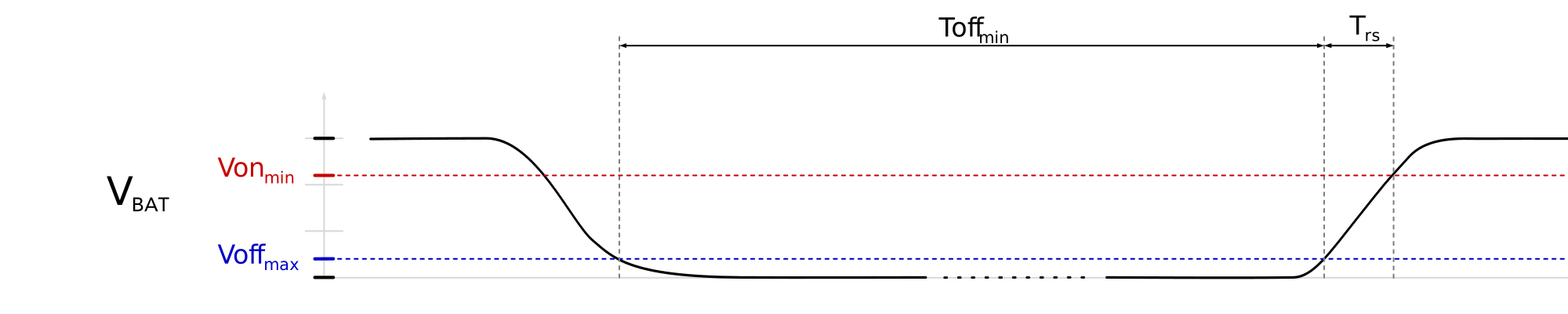
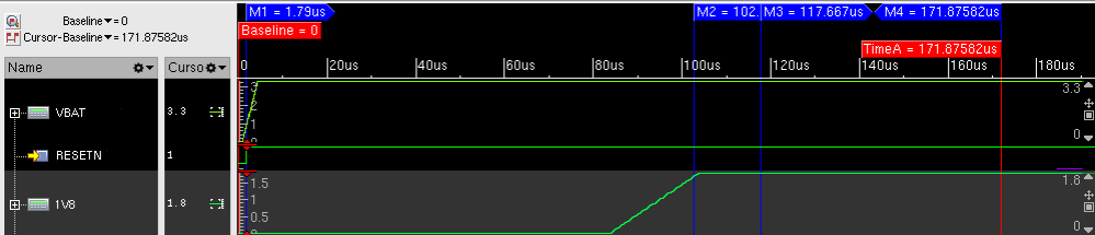
| Name | Description | Min. | Typ. | Max. | Unit |
|---|---|---|---|---|---|
| Vonmin | Minimal ON Voltage | 2.2 | V | ||
| Trs | VBAT Rise Time from Voffmax to Vonmin | 119 | 10 000 | µs |
| Name | Description | Value |
|---|---|---|
| Toffmin @ 50 mV | Minimal OFF (VBAT ≤ Voffmax) time to insure complete reset when Voffmax = 50 mV | 0.1 s |
| Toffmin @ 0.1 V | Minimal OFF (VBAT ≤ Voffmax) time to insure complete reset when Voffmax = 0.1 V | 0.5 s |
| Toffmin @ 0.2 V | Minimal OFF (VBAT ≤ Voffmax) time to insure complete reset when Voffmax = 0.2 V | 1 s |
Power States
Figure 7 represents the electrical states of the module and their transitions.
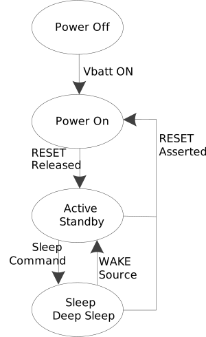
- Active mode: operational, UART on, RF on, LCPU/MCPU/DSP are running. Power consumption depends on workload and transmit power level.
- Standby mode: Same as active mode, except RF off.
- Sleep mode: MCPU/LCPU/DSP are power gated, UART off, RAM content is salvaged. Power level 300 µA circa.
- Deep Sleep Mode: Only the power management unit (PMU) stays active. Power level 1 µA.
More information is given in the table below:
| Power Mode | LTE Mode | Available Interfaces |
|---|---|---|
| Active | Connected (RF on) | All interfaces |
| Standby | Connected (RF off) | All interfaces |
| Sleep | Short eDRX idle duration RRC Idle | WAKE pins (including RTS0/1) |
| Deep Sleep | PSM idle, Long eDRX idle duration, radio-off, airplane | WAKE pins (including RTS0/1) |
PVDD_1V8 BIDIR Pads State in Sleep and Deep Sleep Mode
In Sleep and Deep Sleep mode, the Digital PVDD_1V8 bi-directional I/Os are turned off and behave like 50 MΩ high-impedance pads. Pull-ups / pull-downs are therefore mandatory on output pads to maintain a steady voltage level. Please refer to the EVK reference schematics for an implementation example.
PMU_5V IN Pads State in Deep Sleep Mode
In Deep Sleep mode the digital PMU_5V inputs are turned off and behave like 180 MΩ high-impedance pins.
Table 22 gives the values of the measured leakage current (measurements taken on silicon) for the PMU wake inputs.
| Minimum | Typical | Maximum |
|---|---|---|
| 3 nA | 4 nA | 12 nA |
Table 23 shows values of the external pull-up/pull-down resistor to be used at the PMU wake inputs pads.
| Minimum | Typical | Maximum |
|---|---|---|
| 1 kΩ | 10 kΩ | 100 kΩ |
Table 24 details the PMU wake input pulses detection mechanism timings.
| Maximum pulse width guaranteed to be ignored | Minimum pulse width guaranteed to be recognised |
|---|---|
| 11.1 ns | 100 µs |
Table 25 provides the internal pull-up current range at RESETN.
| Minimum | Typical | Maximum |
|---|---|---|
| 73.5 nA | 100 nA | 160.5 nA |
Digital I/O Characteristics
This section details the voltage and current characteristics of the various I/O pads of the GM02SP.
- PVDD_1V8
- PMU_5V
See Table 26 for the digital I/O characteristics of the different I/O pads. Refer to each interface of the GM02SP in chapter Interfaces for the power group and I/O pad type of each pad. Note that IN pads are inputs only whereas BIDIR can be both inputs and outputs.
| Symbol | Minimum | Maximum | Unit |
|---|---|---|---|
| VIH — Input HIGH level | 1.26 | 3.3 | V |
| VIL — Input LOW level | 0 | 0.54 | V |
| VOH — Output HIGH voltage | 1.44 | 1.8 | V |
| VOL — Output LOW voltage | 0 | 0.36 | V |
| IOH — HIGH level source current | 0 | 220 | mA |
| IOL — LOW level sink current | 0 | 221 | mA |
| IRPU — Input pull-up resistor current | 15 | µA | |
| RRPU — Input pull-up resistance | 27 | 34 | kΩ |
| IRPD — Input pull-down resistor current | 15 | µA | |
| RRPD — Input pull-down resistance | 27 | 34 | kΩ |
| VH — Input hysteresis | 0.18 | V | |
| IPAD — Input leakage current, non-tolerant | -1 | 1 | µA |
| IOZ — Off-State leakage current | 1 | µA |
| Symbol | Minimum | Maximum | Unit |
|---|---|---|---|
| VIH — Input HIGH level | 0.8 | VBAT + 0.6 (max. 5.5) | V |
| VIL — Input LOW level | 0 | 0.2 | V |
RF Performance
It is recommended to add a DC blocking capacitor in series with the module RF input/output pad (#90).
RF Sensitivity
The GM02SP exhibits the following typical RF sensitivity at 2.5 V:
| Band | Typical Sensitivity |
|---|---|
| Low Bands: B5, B8, B12, B13, B14, B17, B18, B19, B20, B26, B28, B85 | -105 dBm |
| High bands: B1, B2, B3, B4, B25, B66 | -106 dBm |
RF Output Power
The GM02SP maximum output power within the recommended operating range (from 2.5 to 5.5 V) is given in Table 29.
| Bands | Output Power |
|---|---|
| All Bands | 23 dBm ± 1 dB |
RF performance at 2.2 V
While it is not recommended to operate the GM02SP in the range 2.2 to 2.5 V, the RF section will continue to work normally, albeit with reduced TX output power as shown in Table 30 below.
| Temperature | Sensitivity Loss | Output Power Loss |
|---|---|---|
| -30 °C | No loss | 1.1 dB |
| 25 °C | No loss | 1.1 dB |
| 85 °C | No loss | 1.7 dB |
Power Supply Dimensioning
This section provides guidance to designers working on the power supply or selecting a suitable battery to power the GM02SP.
Overview
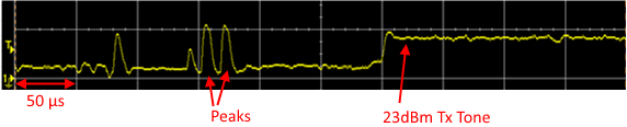
The current consumption of the GM02SP peaks before every TX sub-frame as shown in Figure 8. In this figure, the time division is 50 µs. Around 150 µs from the start, two current pulses peaking 34% higher than the average current consumption during the 23 dBm TX tone which follows can be observed.
Peak Current Measurement Method
- Voltage probes are placed close to module VBAT input.
- Voltage probes accuracy is calibrated using a current probe.
- A large capacitance Cbatt is placed close to the VBAT pin to simulate a battery and screen the device from the parasitic inductances of the cables and tracks.
- 2 × 22 µF capacitors (Cext) are placed between the voltage probes and the module VBAT input to soften the current peaks.
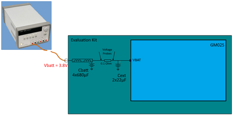
Peak Current Measurement
Table 31 gives the peak current values measured on the setup shown on Figure 9 for different voltages and temperatures.
| Input Voltage | T = -40°C | T = -30°C | T = +25°C | T = +85°C |
|---|---|---|---|---|
| 5.5 V | 328 | 305 | 263 | 268 |
| 3.8 V | 475 | 438 | 444 | 479 |
| 2.5 V | 705 | 667 | 679 | 741 |
| 2.2 V | 676 | 640 | 652 | 717 |
Margin
Module’s Total Capacitance and Inductance
The module’s sum of internal capacitance (positive side tolerance) is 115 µF.
The module’s sum of internal inductance (positive side tolerance) is 5.3 µH.
Maximum Electrical Ratings
| Parameter | Minimum | Maximum |
|---|---|---|
| Supply Voltage VBAT | -0.2 V | 5.5 V |
| I/Os in Power Group PVDD_1V8 | -0.2 V | 4.125 V |
| I/Os in Power Group PMU_5V | -0.2 V | 6.0 V |
Total Capacitance and Inducatance
The total capacitance of the GM02SP is 115 µF. Total inductance is 5.3 µH.
Thermal Considerations
Special attention needs to be given to thermal dissipation.
The outer layers of the host board must be covered in as many wide copper areas as possible, and those must be stitched with evenly spaced ground vias. Care must be taken that no air gap exists along the thermal path from the GM02SP to the dissipating copper area(s). Gaps can be filled with heat conducting materials such as GapPad™.
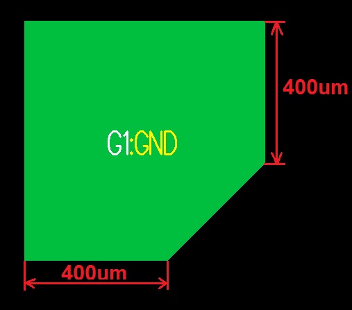
The Gxx pads should be tied to a large ground plane on the customer's PCB layer 1. It is also recommended to have the Gxx pads area on the PCB stitched with through ground vias to improve thermal dissipation.
If the host board is piggybacked over a larger board, the aforementioned heat dissipation considerations should be applied to both the main and the daughter board.
Use the AT command AT+SQNTMON to monitor the current temperature of the modem and
implement alert thresholds. The accuracy of the reported temperature is within ± 3°C.
Mechanical Characteristics
Package Description
The module footprint is (16.3 ± 0.15) mm × (17.0 ± 0.15) mm × 2.30 mm (max.).
See below for the other dimensions.
The GM02SP weighs 1.43 g.
Hardware Module Dimensions
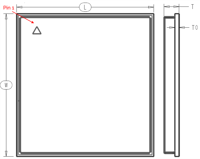
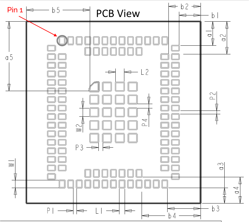
| Dimension | Value (mm) |
|---|---|
| L | 16.3 ± 0.15 |
| W | 17.0 ± 0.15 |
| T | 2.3 max (2.2 typical) |
| T0 | 0.8 max |
| L1 | 0.5 ± 0.1 |
| W1 | 0.7 ± 0.1 |
| L2 | 0.8 ± 0.1 |
| W2 | 0.8 ± 0.1 |
| a1 | 2.25 ± 0.1 |
| a2 | 3.05 ± 0.1 |
| a3 | 1.45 ± 0.1 |
| a4 | 2.45 ± 0.1 |
| a5 | 6.5 ± 0.1 |
| b1 | 2.0 ± 0.1 |
| b2 | 3.0 ± 0.1 |
| b3 | 3.1 ± 0.1 |
| b4 | 5.5 ± 0.1 |
| b5 | 5.95 ± 0.1 |
| P1 | 0.3 ± 0.1 |
| P2 | 0.3 ± 0.1 |
| P3 | 0.4 ± 0.1 |
| P4 | 0.4 ± 0.1 |
Laser Marking
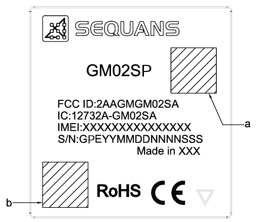
- The triangle in the bottom-right corner provides pin #1 location.
- FCC ID: 2AAGMGM02SA
- IC: 12732A-GM02SA
- IMEI:XXXXXXXXXXXXXXX
- S/N:GPEYYMMDDNNNNSSS (16 digits)
- GPE: reserved, value subject to change at Sequans’s discretion (3 digits);
- YYMMDD: Manufacturing Date (YY:Year;MM:Month,DD:Day);
- NNNN: Panel counter (from 0001~9999);
- SSS: Piece location on panel (from 001~036)
- 2D marked “a” refer to IMEI Barcode
- 2D marked “b” refer to S/N Barcode
- XXX represents the country of origin, and can be either PRC for China or VN for Vietnam.
Environmental Conditions
Packing
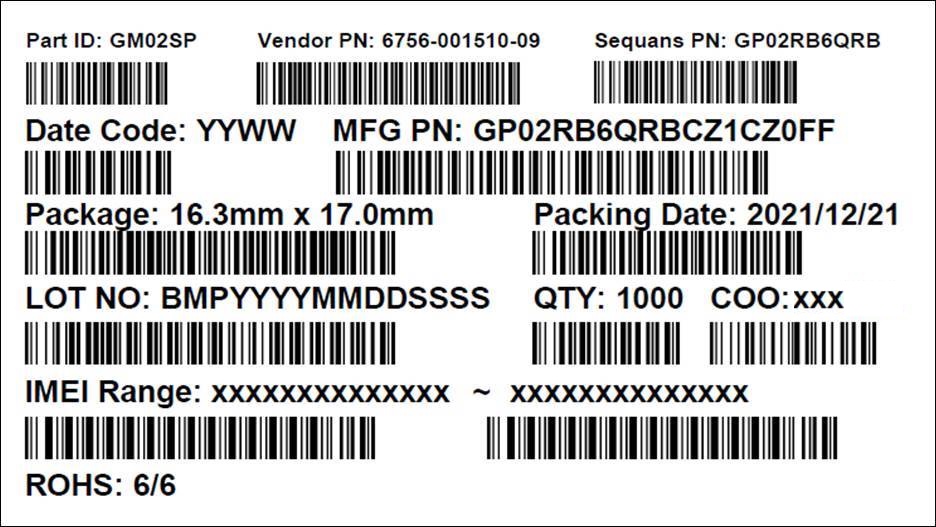
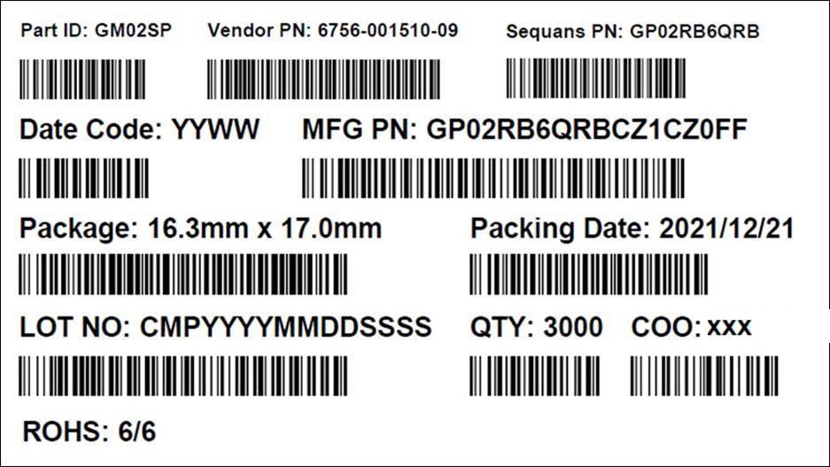
The GM02SP is delivered in Tape-and-Reel. Details are provided in the figures below.
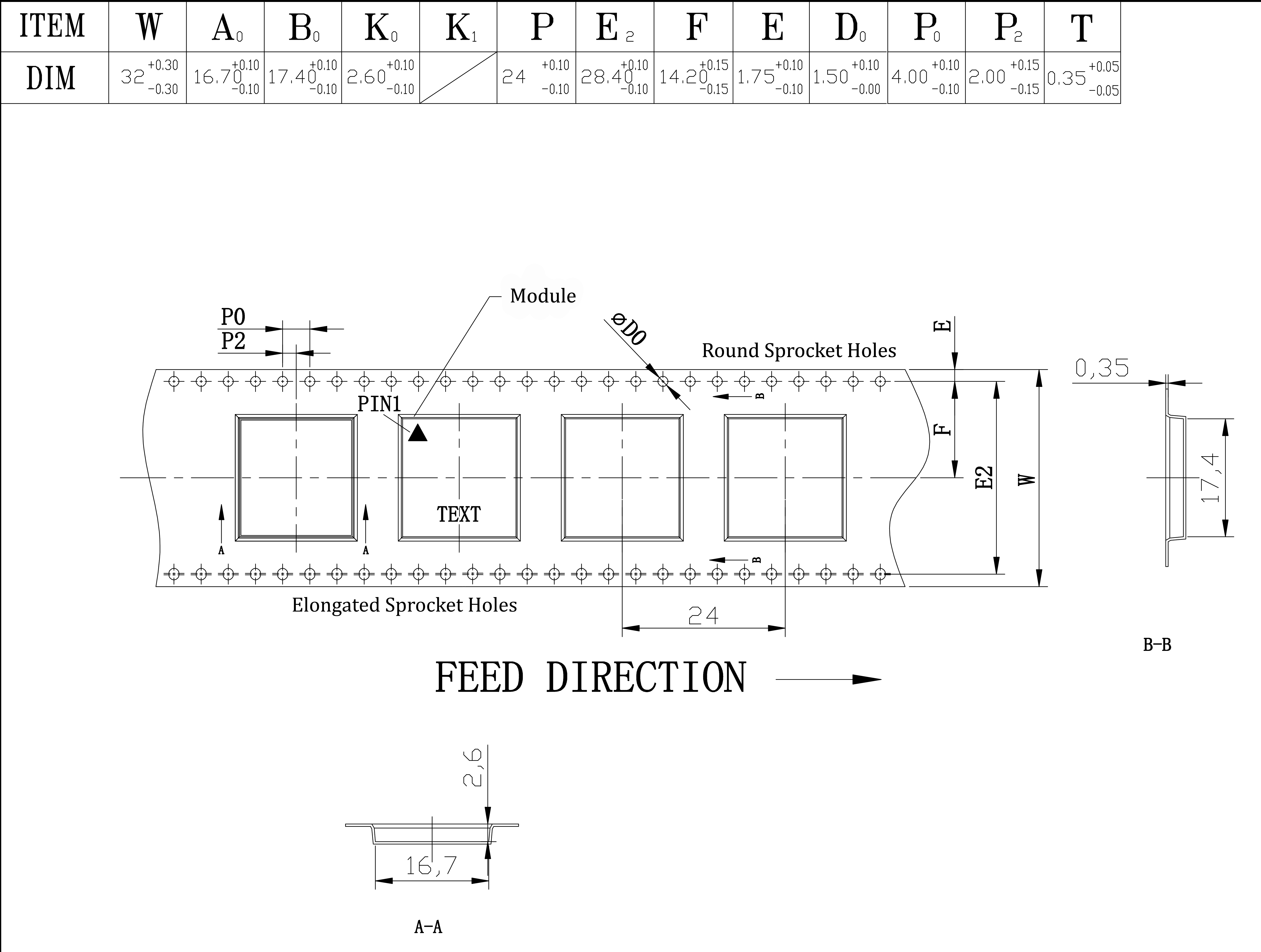
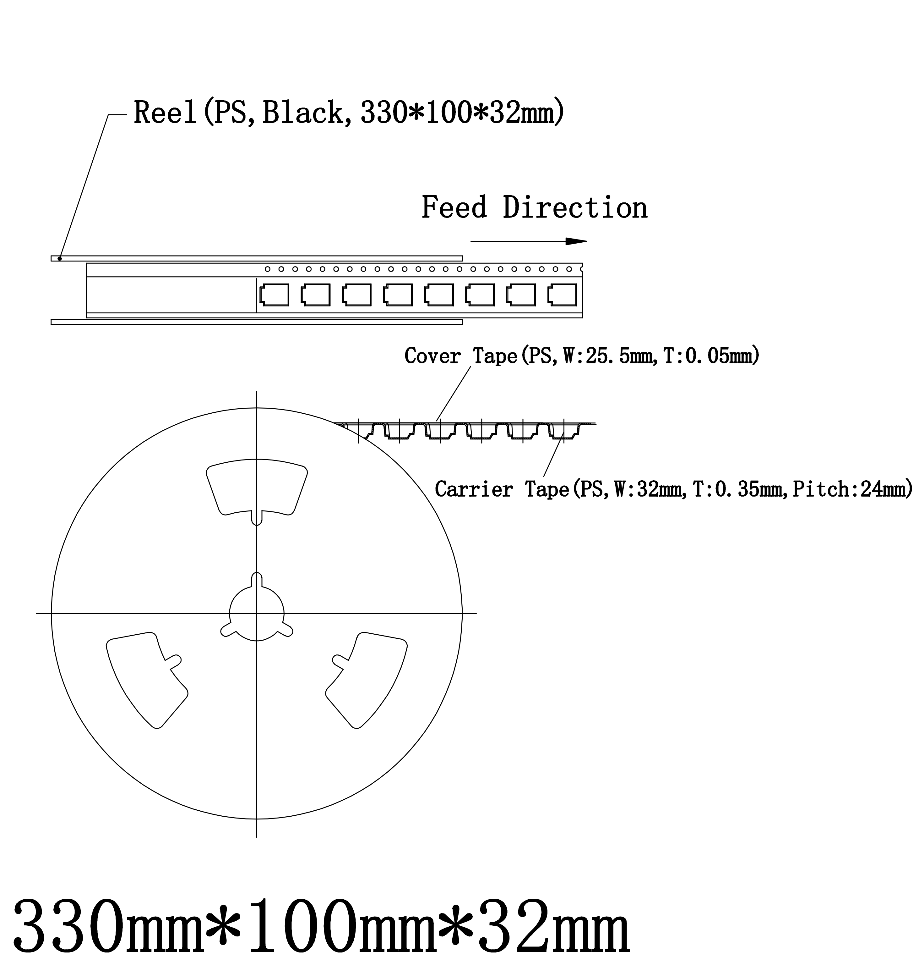
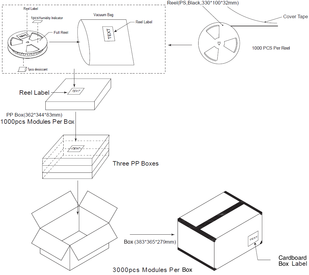
The full box set weights about 5.95 kg.
Storage and Mounting
The GM02SP module is Moisture Level 3 rated as per JEDEC industrial standard.
The GM02SP is JEDEC J-STD-033D compliant and can be stored at T < 40 °C and relative humidity < 90%.
The GM02SP can withstand up to three reflows at a maximum of 245°C.
| Profile Feature | |
|---|---|
| Solder Paste Alloy | Sn 96.5/Ag 3.0/Cu 0.5 (Lead Free solder paste) |
| Peak Package Body Temperature | 235 °C to 245 °C |
| Fusion Time |
Temp: 217 to 245 °C Duration: 60 to 90 s |
| Pre-heat / Soak |
Temp: 150 to 217 °C Time: 90 to 120 s |
| Ramp-up Rate | < 3 °C/s |
| Ramp-down Rate | -3 to 0 °C/s |
| Air composition | N2, O2 contents less than 1,500 ppm |
Recommended stencil thickness: 0.12 to 0.13 mm, to allow for enough solder paste and avoid risks of dry soldering and wrapage issues.
Following reflow soldering, the GM02SP can be washed with deionised RO water to remove any remaining flux. The module then needs a single backing at 125 °C during 16 hours. The module's package may be slightly discoloured during baking.
Reliability Specifications for Hardware Rev. 3
The GM02SP has been tested against Sequans's industrial reliability specification as described in Table 36.
| Item | Test conditions | Standard | #Samples | Result |
|---|---|---|---|---|
| Preconditioning |
(a) Bake: 125°C / 24 hours (b) MSL3: 30°C/60% RH, 192 hrs (c) SAT (CSAM & TSCAN) (d) X-ray (e) Reflow 3 cycles at Tp: 250 ±2°C (f) SAT (CSAM & TSCAN) |
JESD22-A113 | 225 | PASS |
| TC |
Temperature Shock Cycling (TC): -40°C to +85°C air to air, 20 minutes, ramp rate 20°C/minute, 1000 cycles |
JESD22-A104 | 25 | PASS |
| THB |
Temperature Humidity Bias Test +85°C, 85 % RH, Vcc Max, Read Point at 168/500/1,000 hrs |
JESD22-A101 | 25 | PASS |
| HAST |
|
JESD22-A110 | 25 | PASS |
| Environmental Testing - A Cold |
Environmental Testing Test A Cold. -40°C, 500 hrs |
IEC60068-2-1 JESD22-A119 | 25 | PASS |
| Environmental Testing - B Dry Heat |
Environmental Testing Test B Dry Heat. +85°C, 500 hrs |
IEC60068-2-2 JESD22-A103 | 25 | PASS |
| HTOL |
High Temperature Operating Test 85 °C, Vcc max, Tx: 50% / Rx: 50%. Read Point at 283/500/1,000 hrs |
N/A | 50 | PASS |
| LTOL |
Low Temperature Operating Test <50 °C, Vcc max, Tx: 50% / Rx: 50%. Read Point at 283 hrs |
JESD22-A108 | 25 | PASS |
| High Temperature Storage Test (HST) | 150 °C/1,000 hours | JESD22-A103 | 25 | PASS |
| Intermittent Operating Life (IOL) |
|
N/A | 25 | PASS |
| Power and Temperature Cycling | Test Condition A – -40 to +85 °C | JESD22-A105 | 25 | PASS |
| Shock |
Mechanical Shock (MS) (Half Sine, 500G, 1.0 ms, 1 shock for each ±axis) |
DIN IEC 68-2-27 | 15 | PASS |
| Drop |
Drop Test:
|
DIN IEC 68-2-31 ETS 300019-2-7 | 15 | PASS |
| Vibration |
Vibration Test (Vib) Sweep-Sine Vibration. Sinusoidal, 10 ~ 500 Hz, 1.0 octave/min, 10 sweep cycles for 2 hr for each axis. |
DIN IEC 68-2-6 EIA/TIA 571 §4.1.1.2 | 15 | PASS |
| ESD | HBM Start: ±1000V, Stop:± 1500V | JS-001JESD22-A114 | 12 | PASS |
| CDM Start: ±250V, Stop: ±500V | JS-002STM5.3.1 | 12 | PASS | |
| TCT |
Temperature Change Test 10 cycles; 1 cycle has the following steps (roughly 7+ hrs):
|
IEC60068-2-14 | 25 | PASS |
Mean Time To Failure (MTTF)
- There was no failure recorded on a cumulative Dh=50,000 hour run (50 devices tested for 1000 hours), which, at a confidence level of 60%, results in a failure rate Fr equal to 0.93.
- Stress test temperature Ts is 75 °C.
- The thermal activation energy Ev is assumed to be 0.7 eV.
Considering the figures given above, the resulting MTTF for the GM02SP at 60% confidence level and a usage temperature Tu of 25°C is 313 years. At a usage temperature Tu of 55°C, this figure drops to 25.9 years.
GNSS Characteristics
| Generic Features | Comments |
|---|---|
| GPS Constellation Support | L1 band |
| On-device GNSS navigation mode, using satellite broadcast ephemerides and almanac | Not recommended for low power consumption; back-up mode when no GNSS cloud assistance is available |
| Assisted on-device GNSS navigation mode using live assistance (Ephemerides) downloaded from the cloud |
|
| Three choices of RF capture lengths: short, medium and long | Flexible trade-off between sensitivity, accuracy, time to first fix and power consumption constraints |
| Specific Features Support with Partner | Comments |
|---|---|
| On-device GNSS pre-processing mode, followed by on-cloud final navigation |
|
| Application Features | Comments |
|---|---|
| Non-concurrent LTE Tx/Rx with GNSS processing | GNSS fix can be acquired when AT+CFUN=0 or
AT+CFUN=4 |
| Concurrent support of GNSS with PSM mode | As long as the PSM exit timer is not expected to fire within the next 120 s. |
| Performance | Comments |
|---|---|
|
Sensitivity (lab; open-sky conditions and long RF capture):
|
|
|
Accuracy (lab; open-sky conditions and long RF capture):
Accuracy (live condition; antenna with full sky visibility and long RF capture)
|
|
|
Time-To-First-Fix (lab; open-sky conditions & all RF capture lengths)
|
Regulatory Approval
FCC Regulatory Approval
FCC-ID: 2AAGMGM02SA (single modular approval)
FCC-ID: 2AAGMG02SA (single modular approval)
Changes or modifications not expressly approved by the party responsible for compliance could void the user’s authority to operate the equipment.
This device complies with parts 22/24/27/90 of the FCC Rules.
- This device may not cause harmful interference.
- This device must accept any interference received, including interference that may cause undesired operation.
Installation/Integration
This above identified radio module is not intended to be provided to end-users but is for installation by OEM integrators only.
Sequans's module integration guidelines must be closely followed.
Compliance of host integrations of the module is limited to hosts adaptation designs which are identical to Sequans' reference design.
Host integrations with adaptation designs deviating from Sequans' reference design require either filing a Class 2 Permissive Change to this modular approval or separate approval for the end-Product under its own FCC ID.
Host integrations with co-located (simultaneously operating) radio transmitters must be evaluated in accordance with FCC multi-transmitter rules and may require either filing a Class 2 Permissive Change to this modular approval or separate approval for the end-Product under its own FCC ID. Dependent on the result of the evaluation.
An inquiry to the FCC or a TCB is urgently recommended.
Antennas
This radio transmitter has been tested and approved by the FCC to operate with the antennae listed below:
- Aaronia AG OmniLOG® 90200 – max. antenna gain = 2 dBi.
- Fractus Antennas TRIO mXTEND™ (FR01-S4-210) – max. antenna gain = 2.4 dBi.
| Band | Frequency range (MHz) | Maximum Antenna Gain (dBi) |
|---|---|---|
| B2 | 1850 – 1910 | 8.0 |
| B4 | 1710 – 1755 | 5.0 |
| B5 | 824 – 849 | 9.4 |
| B8 | 897.5 - 900.5 | 9.77 |
| B12 | 699 – 716 | 8.6 |
| B13 | 777 – 787 | 9.1 |
| B17 | 704 – 716 | 8.7 |
| B25 | 1850 – 1915 | 8.0 |
| B26 | 814 – 849 | 9.4 |
| B66 | 1710 – 1780 | 5.0 |
| B85 | 698 – 716 | 8.6 |
The use of an antenna having a gain greater than the above indicated in any of those specified bands is strictly prohibited.
RF Exposure Safety
This module complies with the FCC RF exposure limits and has been evaluated in compliance with mobile exposure conditions.
The equipment must be installed and operated with minimum distance of 20 cm of the human body.
End-Product RF Exposure Safety
Integrations of this module into end-products which are intended for portable use, i.e. less than 20 cm distance between its radiating structures (antenna) and the body of nearby persons, or which otherwise put additional technical requirements, like Hearing Aid compatibility, require either filing a Class 2 Permissive Change to this modular approval or separate approval for the end-Product under its own FCC ID.
Compliance with FCC Rule Part 15B
Note: This equipment has been tested and found to comply with the limits for a Class B digital device, pursuant to part 15 of the FCC Rules. These limits are designed to provide reasonable protection against harmful interference in a residential installation. This equipment generates, uses and can radiate radio frequency energy and, if not installed and used in accordance with the instructions, may cause harmful interference to radio communications. However, there is no guarantee that interference will not occur in a particular installation. If this equipment does cause harmful interference to radio or television reception, which can be determined by turning the equipment off and on, the user is encouraged to try to correct the interference by one or more of the following measures:
- Reorient or relocate the receiving antenna.
- Increase the separation between the equipment and receiver.
- Connect the equipment into an outlet on a circuit different from that to which the receiver is connected.
- Consult the dealer or an experienced radio/TV technician for help.
End-product Compliance with FCC Rule Part 15B (Unwanted Emission Limits for Digital Device)
If the OEM of the end-product fully complies with the above described reference design, they can inherit and rest on the existing modular approval for RF compliance.
The OEM of the end-product remains still responsible to show compliance of the overall end-product with the FCC limits for unwanted conducted and radiated emissions from the digital device (unintentional radio) portion of such end-product (commonly addressed as part 15B compliance or similar).
End-Product Labelling
The module's FCC ID must either be visible from the exterior of the end-product (e.g. per window) or per electronic display, or shall be displayed on an additional exterior label per the following or similar string:
Contains FCC ID: 2AAGMGM02SA
Contains FCC ID: 2AAGMG02SA
Further labelling requirements may apply depending on the FCC rule parts relevant to the end-product.
End-product User manual
The OEM integrator has to be aware not to provide information to the end user regarding how to install or remove this RF module in the user's manual of the end product which integrates this module.
The user manual of the end-product shall include all the applicable regulatory information/warnings.
ISED Regulatory Approval (English)
Changes or modifications not expressly approved by the party responsible for compliance could void the user’s authority to operate the equipment.
This device complies with ISED Radio Standards Specifications RSS-130, RSS-132, RSS-133, RSS-139.
Installation/Integration
This above identified radio module is not intended to be provided to end-users but is for installation by OEM integrators only. The integration guidelines must be closely followed.
Compliance of host integrations of the module is limited to hosts adaptation designs which are identical to the reference design.
Host integrations with adaptation designs deviating from the reference design require either filing a Class 2 Permissive Change to this modular approval or separate approval for the end-Product under its own IC.
Host integrations with co-located (simultaneously operating) radio transmitters must be evaluated in accordance with ISED multi-transmitter rules and may require either filing a Class 2 Permissive Change to this modular approval or separate approval for the end-Product under its own IC. Dependent on the result of the evaluation.
An inquiry to the ISED or an FCB is urgently recommended.
Antennas
This radio transmitter has been tested and approved by the ISED to operate with the antennae listed below:
- Aaronia AG OmniLOG® 90200 – max. antenna gain = 2 dBi.
- Fractus Antennas TRIO mXTEND™ (FR01-S4-210) – max antenna gain = 2.4 dBi.
To comply with both the ISED maximum EIRP limits and with RF Exposure rules, the maximum antenna gain for the operation bands are:
| Band | Frequency Range (MHz) | Maximum Antenna Gain (dBi) |
| B25 | 1850 – 1915 | 8.0 |
| B2 | 1850 – 1910 | 8.0 |
| B66 | 1710 – 1780 | 5.0 |
| B4 | 1710 – 1755 | 5.0 |
| B5 | 824 – 849 | 6.1 |
| B85 | 698 – 716 | 5.6 |
| B12 | 699 – 716 | 5.6 |
| B17 | 704 – 716 | 5.6 |
| B13 | 777 – 787 | 5.9 |
The use of an antenna having a gain greater than the above indicated in any of those specified bands is strictly prohibited.
RF exposure safety
This module complies with the ISED RF exposure limits and has been evaluated in compliance with mobile exposure conditions.
The equipment must be installed and operated with minimum distance of twenty centimetres of the human body.
End-product RF exposure safety
Integrations of this module into end-products which are intended for portable use, i.e. less than 20 cm distance between its radiating structures (antenna) and the body of nearby persons, or which otherwise put additional technical requirements, like Hearing Aid compatibility, require either filing a Class 2 Permissive Change to this modular approval or separate approval for the end-Product under its own IC.
Compliance with Interference-Causing Equipment Standard
This Class B digital apparatus complies with ISED’s Interference-Causing Equipment Standard ICES-003.
End-product compliance with Interference-Causing Equipment Standard
If the OEM of the end-product fully complies with the above described reference design, they can inherit and rest on the existing modular approval for RF compliance.
The OEM of the end-product remains still responsible to show compliance of the overall end-product with the applicable Interference-Causing Equipment Standards issued by the ISED.
End-product Labelling
The module's IC must either be visible from the exterior of the end-product (e.g. per window) or per electronic display, or shall be displayed on an additional exterior label per the following or similar string:
Contains IC: 12732A-GM02SA
Further labelling requirements may apply depending on the applicability of other Radio Standard Specifications relevant to the end-product.
End-product User manual
The OEM integrator has to be aware not to provide information to the end user regarding how to install or remove this RF module in the user's manual of the end product which integrates this module.
The user manual of the end-product shall include all the applicable regulatory information/warnings.
Pending.
Autorisation Réglementaire de l'ISDE (Français)
Les changements ou modifications non expressément approuvés par la partie responsable de la conformité peuvent annuler l'autorisation de l'utilisateur à utiliser l'équipement.
Cet appareil est conforme aux spécifications des normes radio ISDE RSS-130, RSS-132, RSS-133, RSS-139.
Installation/Intégration
Le module radio identifié ci-dessus n'est pas destiné à être fourni aux utilisateurs finaux, mais est destiné à être installé uniquement par des intégrateurs OEM. Les directives d'intégration doivent être suivies à la lettre.
La conformité des intégrations hôtes du module est limitée aux conceptions d'adaptation des hôtes qui sont identiques à la conception de référence.
Les intégrations hôtes avec des conceptions d'adaptation s'écartant de la conception de référence nécessitent soit le dépôt d'une modification permissive de classe 2 à cette approbation modulaire, soit une approbation distincte pour le produit final sous son propre CI.
Les intégrations hôtes avec des émetteurs radio colocalisés (fonctionnant simultanément) doivent être évaluées conformément aux règles multi-émetteurs ISDE et peuvent nécessiter soit le dépôt d'une modification permissive de classe 2 à cette approbation modulaire, soit une approbation distincte pour le produit final sous son propre CI. Cela dépend du résultat de l'évaluation.
Une demande de renseignements auprès de l'ISDE ou d'un FCB est recommandé de toute urgence.
Antennes
Cet émetteur radio a été testé et approuvé par l'ISDE pour fonctionner avec les antennes énumérées ci-dessous :
• Aaronia AG OmniLOG® 90200 – gain d'antenne maximal = 2 dBi
• Fractus Antennas TRIO mXTEND™ (FR01-S4-210) – gain d'antenne maximal = 2,4 dBi
Pour se conformer aux limites EIRP maximales de l'ISDE et aux règles d'exposition aux fréquences radio, le gain d'antenne maximal pour les bandes de fonctionnement est :
| Bande | Limites de bande (MHz) | Gain maximal d'antenne (dBi) |
|---|---|---|
| B25 | 1850 – 1915 | 8.0 |
| B2 | 1850 – 1910 | 8.0 |
| B66 | 1710 – 1780 | 5.0 |
| B4 | 1710 – 1755 | 5.0 |
| B5 | 824 – 849 | 6.1 |
| B85 | 698 – 716 | 5.6 |
| B12 | 699 – 716 | 5.6 |
| B17 | 704 – 716 | 5.6 |
| B13 | 777 – 787 | 5.9 |
L'utilisation d'une antenne ayant un gain supérieur à celui indiqué ci-dessus dans l'une des bandes spécifiées est strictement interdite.
Sécurité d'exposition aux RF
Ce module est conforme aux limites d'exposition aux RF de l'ISDE et a été évalué conformément aux conditions d'exposition mobile.
L'équipement doit être installé et utilisé à une distance minimale de 20 cm du corps humain.
Sécurité d'exposition aux RF du produit final
L'intégration de ce module dans des produits finaux destinés à une utilisation portable, c'est-à-dire à une distance inférieure à 20 cm entre ses structures rayonnantes (antenne) et le corps des personnes à proximité, ou qui imposent des exigences techniques supplémentaires, comme la compatibilité avec les prothèses auditives, nécessite soit le dépôt d'une modification permissive de classe 2 à cette approbation modulaire, soit une approbation distincte pour le produit final sous son propre CI.
Conformité aux normes sur le matériel brouilleur
Cet appareil numérique de classe B est conforme à la norme NMB-003 de l'ISDE sur les équipements brouilleurs.
Conformité du produit final à la norme sur les équipements brouilleurs
Si le fabricant d'équipement d'origine du produit final est entièrement conforme à la conception de référence décrite ci-dessus, il peut hériter et s'appuyer sur l'approbation modulaire existante pour la conformité RF.
Le fabricant d'équipement d'origine du produit final reste toujours responsable de démontrer la conformité du produit final global aux normes applicables sur les équipements brouilleurs émises par l'ISDE.
Étiquetage du produit final
Le circuit intégré du module doit être visible de l'extérieur du produit final (par exemple, par fenêtre) ou par affichage électronique, ou doit être affiché sur une étiquette extérieure supplémentaire conformément à la chaîne suivante ou similaire :
Contient le circuit intégré : 12732A-GM02SA
D'autres exigences d'étiquetage peuvent s'appliquer en fonction de l'applicabilité d'autres spécifications de normes radio pertinentes pour le produit final.
Manuel d'utilisation du produit final
L'intégrateur OEM doit veiller à ne pas fournir d'informations à l'utilisateur final concernant la manière d'installer ou de retirer ce module RF dans le manuel d'utilisation du produit final qui intègre ce module.
Le manuel d'utilisation du produit final doit inclure toutes les informations/avertissements réglementaires applicables.
ACMA Regulatory Marking

RE-D Regulatory Safety Notice
UKCA Regulatory Marking

Acronyms
| Acronym | Definition |
|---|---|
| ADC | Analogue to Digital Converter |
| CPU | Central Processing Unit |
| DL | Downlink |
| ESD | Electro-static discharge |
| GND | Ground |
| GNSS | Global Navigation Satellite System |
| GPIO | General Purpose Input Output |
| GPS | Global Positioning System |
| I/O | Input/Output |
| I²C | Inter-Integrated Circuit interface |
| IMEI | International Mobile Equipment Identity |
| IP | Internet Protocol |
| JTAG | Joint Test Action Group |
| LGA | Large Grid Array |
| LNA | Low-Noise Amplifier |
| GNSS | Global Navigation Satellite System |
| LTE | Long Term Evolution, or 4G. Standard is developed by the 3GPP. |
| MIMO | Multiple In Multiple Out |
| NAS | Network Access Server |
| PCM | Pulse-Code Modulation |
| PHY | Physical Layer |
| RED | European Radio Equipment Directive |
| SAW | Surface Acoustic Wave (filter) |
| RF | Radio Frequency |
| RoHS | Restriction of Hazardous Substances |
| Rx | Reception |
| S/N | or SN: Serial Number |
| SIM | Subscriber Identification Module |
| SMS | Short Message Service |
| SPI | Serial Peripheral Interface |
| Tx | Transmission |
| UART | Universal Asynchronous Receiver Transmitter |
| UE | User Equipment |
| UL | Uplink |
| USB | Universal Serial Bus |